
06_pixel_assembly.md 42 KB
title: Phase I Silicon Detector Assembly ...
The CMS Phase I Upgrade project was a successful effort to design and construct an improved detector for Run 2 of the LHC. In particular, both the forward and barrel sections of the pixel detector were replaced with a redesigned and upgraded version to effectively handle the higher instantaneous luminosity conditions of Run 2. The upgraded pixel detector was installed in early 2017 and has operated well for data taking in 2017 and 2018. This chapter will describe contributions made by the team at UNL to the design, testing, and assembly of modules for the forward section of the pixel detector upgrade. The author of this work contributed significantly to the design and construction of the assembly tooling, and wrote the software that controlled that tooling. In addition, the author designed and partially implemented a high performance telescope for future test beam studies.
CMS Pixel Detector Upgrade
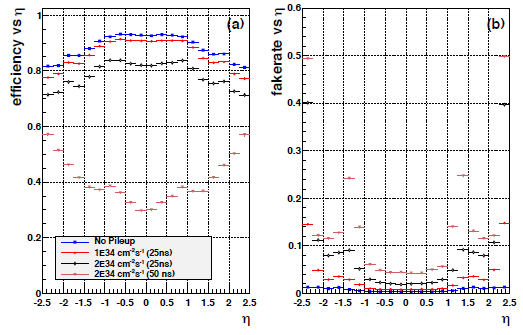
The original CMS pixel detector was designed to record three 3D positions of charged particles as they leave the luminous region as long as they are within $|\eta|<2.5$. It could do this reliably for bunch crossings coming every 25 ns with an average number of pileup interactions of up to 25, equivalent to an instantaneous luminosity of $1\times10^{34}$ $\mathrm{cm}^{-2}\mathrm{s}^{-1}$. However, increasing the instantaneous luminosity higher than this dramatically reduces the efficiency of the detector due to buffer overruns and sensor degradation from more radiation exposure. [@Fig:phase_0_performance] demonstrates how the performance suffers as the number of pileup interactions grows.
 {#fig:phase_0_performance}
To address this problem, a new pixel detector was designed. The new design incremented the number of barrel layers from three to four and the number of forward layers from two to three. It also utilized the new PSI46 readout chip with digital readout, and very low mass construction, important for minimizing the number of radiation lengths in the tracker. Like the original detector, it uses 100$\mu\mathrm{m}$ by 150$\mu\mathrm{m}$ pixels. [@Fig:tracker_compare] shows a comparison between the geometries of the original and upgraded pixel detector.
![]() {#fig:tracker_compare}
{#fig:tracker_compare}
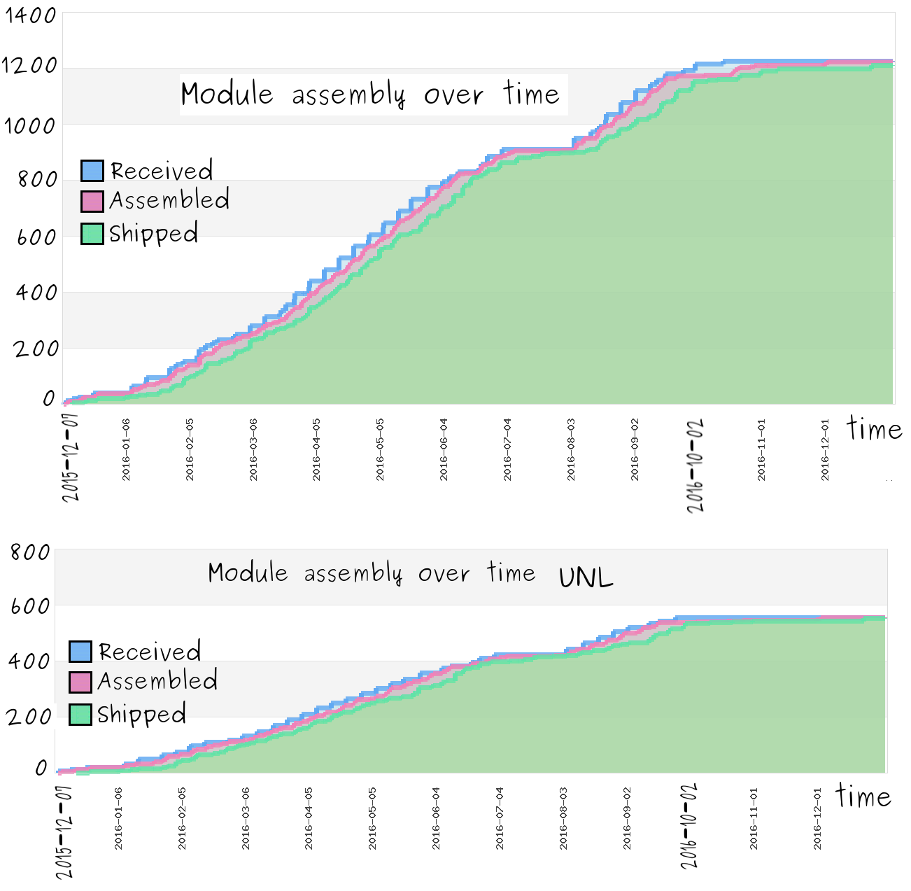
The construction of the barrel and endcap sections of the upgraded pixel detector was split into separate projects. UNL collaborated with several other US institutes to build the forward section. The task of module assembly was divided between the two construction sites: UNL and Purdue University. Module testing was done at the University of Kansas and at FNAL, and the integration facility was also at FNAL. [@Fig:assembly_progress] shows the total number of modules assembled over time for both assembly sites, and for UNL only. In total 1224 were assembled and shipped to the integration site, 555 of them from UNL.
 {#fig:assembly_progress}
The FPIX module consists of several discrete parts, shown in [@fig:module]. These are the silicon sensor, sixteen readout chips (ROCs), a high-density interconnect (HDI) flex circuit, and the token-bit manager (TBM). The sensor and ROCs are electrically and mechanically connected via a grid of indium bump-bonds that allow for charge liberated in the sensor to be collected by the pixels on the ROCs. This process is done by a specialized vendor, so the sensor and ROCs come to the assembly sites as a single unit called a bump-bonded module (BBM). The high density interconnect (HDI) circuit also arrives to the assembly site preassembled with the token bit manager (TBM) chip and several passive elements already attached. The TBM coordinates the readout of the 16 ROCs into a single digital readout signal. Having these two parts, the necessary steps to produce a finished module are:
- Glue the HDI to the sensor side of the BBM.
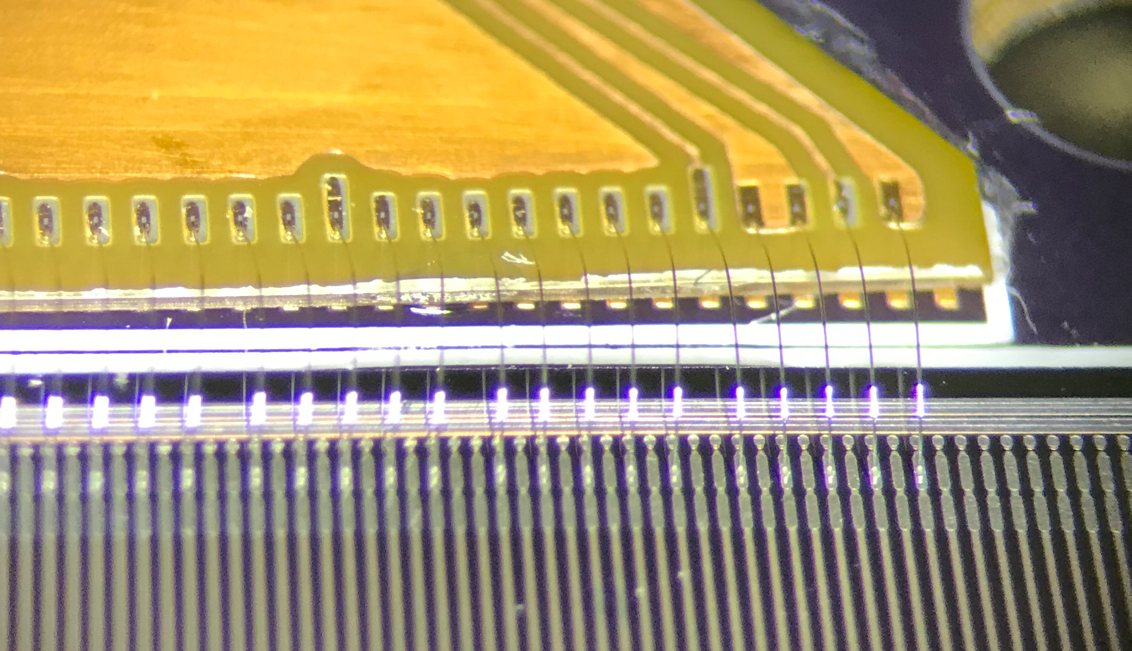
- Wirebond the HDI to the ROCs, the TBM to the HDI, and the bias voltage on the HDI to the silicon sensor. [@Fig:wirebonds] shows wirebonds representative of those used in module construction.
- Encapsulate the wirebonds made in step 2. The encapsulation process helps protect the wirebonds from electric shorts and dampen oscillations resulting from transient currents in CMS's strong magnetic field.
 {#fig:module width=80%}
 {#fig:wirebonds}
After a module has been assembled, functional testing is done to ensure that the ROCs are all operational and the sensor has adequate performance. The flow of these steps is described in [@fig:assembly_flow]. The assembly flow was designed to be a pipeline where multiple batches of modules can be flowing through the process simultaneously; e.g. a batch of modules can be being glued at the same time that a previous batch is being wirebonded.
 {#fig:assembly_flow}
The gluing and encapsulation steps employed a high-precision robotic gantry, shown with tooling in [@fig:gantry]. The gantry was controlled by a custom LabVIEW application, discussed in more detail in the next section.
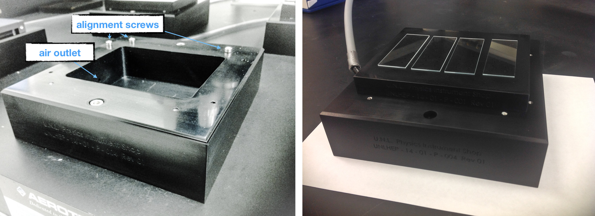
The gantry table has an arrangement of eight "chucks" ([@fig:chucks]). These are identical except for the HDI chuck and one of the BBM chucks which have four individually controlled vacuum lines each, as opposed to the rest which have a single vacuum line for the entire chuck. Each chuck holds one of several types of "plates". Each plate has four positions that serve to align parts used in assembly. The vacuum on the chucks serves two purposes. First, it serves to hold the plate fixed during the assembly process, and second, for the HDI and BBM plates, it supplies vacuum to hold the HDI or BBM fixed on the plate. The HDI and BBM plates have thin precision-cut pieces of metal called stencils glued to their top face. These stencils are used to consistently position the HDI or BBM on the plates.
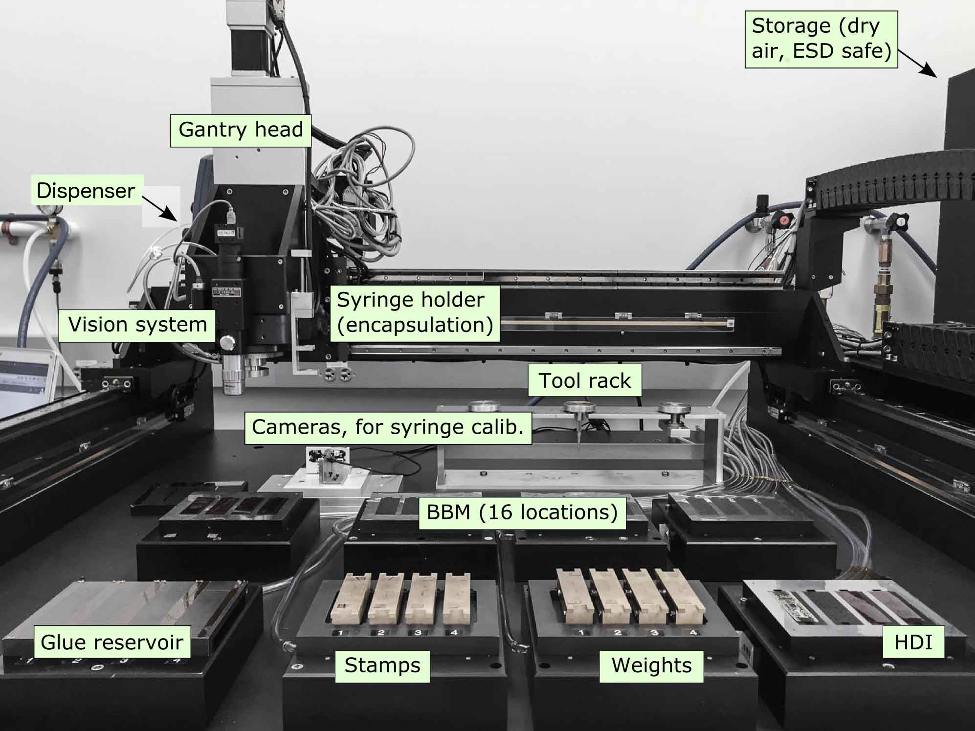 {#fig:gantry}
The gantry head has an adapter plate which allows it to interface with and pickup various tools that are stored on the tool rack. There are two tools used in the gluing procedure: the "picker tool" and the "grabber tool". The grabber tool has metal fingers that fit underneath the tabs on the stamps and weights to lift them and move them around the gantry table. The picker tool has two small suction cups that can be supplied with vacuum to pick up the HDI so it can be placed on a BBM.
The gluing procedure is as follows:
- Place up to four BBMs on a designated BBM chuck; for example the top left chuck in [@fig:gantry].
- Place a matching number of HDI on the designated HDI chuck.
- Place the stamps and weights onto their appropriate chuck, as shown in [@fig:gantry].
- Turn on the vacuum supply to all chucks.
- Use the camera on the gantry head to acquire the position of the fiducial markings on the HDI and BBM. Perform a fit based on those measurements to acquire the exact center and orientation of the parts in gantry coordinates.
- Prepare the Araldite 2011 epoxy and deposit enough into the glue reservoir to create an even layer level with the top of the reservoir.
- Acquire the grabber tool from the tool rack, use it to lift a stamp, and dip it in glue. Place the stamp onto the BBM, using the weight of the stamp itself to apply the glue. Return the stamp to the stamp chuck.
- Return the grabber tool and acquire the picker tool. Use it to lift the HDI and place it on the BBM, using the precision measurements from step 5 to ensure that there is no offset or rotation between the two parts.
- Return the picker tool and get the grabber tool again. Use it to lift a weight and place it onto the BBM-HDI assembly.
- Return the grabber tool to the tool rack. Repeat steps 7-9 for the remaining modules.
 {#fig:chucks}
The encapsulation routine is in many ways simpler than the gluing one. It is performed by filling a syringe with a silicone elastomer called Sylgard. The needle on the syringe is mounted on the gantry head which brings it to just slightly above the wirebonds. A precision fluid dispenser unit then applies pressurized air to the syringe, forcing the Sylgard out of the needle tip. The gantry simultaneously moves slowly across a group of wirebonds to deposit the desired amount of Sylgard. When freshly mixed, the Sylgard has middling viscosity similar to room temperature honey. However, as time pases the Sylgard begins to cure and its viscosity increases. To compensate for this, the speed as which the needle moves is decreased as time-since-mixing grows.
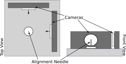
One challenge to encapsulation is the need for precise knowledge of the needle-tip offset. Specifically, one needs to know the vector offset between the point in focus directly underneath the gantry-head camera and the tip of the encapsulation needle, and this offset needs to be recalibrated each time a new needle is loaded due to slight bends and small manufacturing defects in the needles. To acquire the offset, a duel-camera setup was deployed. It consisted of two cameras placed at right angles with an inverted needle placed where their two focal planes intersect ([@fig:needle_calibration]). This is used by first bringing the gantry head camera to the setup, then centering and focusing on the tip of the inverted needle. The gantry coordinates at this position are recorded. Next, the encapsulation needle on the gantry head is brought to close proximity with the inverted needle. The two cameras on the setup are used to guide the operator to align the two needle tips so they are just touching. The difference between this position and the previous recorded position is the vector offset needed for needle-tip calibration.
 {#fig:needle_calibration}
Automated Assembly of FPIX Modules
During module pre-production the first version of the LabVIEW gantry control application was written. As an R&D platform, the initial software served to develop the procedures and tooling for module assembly outlined in the previous section. However, as the project moved into production, serious flaws in the design of the software became apparent. Specifically, a memory leak in the encapsulation routine rendered the software unable to encapsulate batches of more than 1 module. This resulted in each module taking roughly an hour to encapsulate, straining the limited manpower available at UNL. The operation of the software also required significant training, further taxing the team. These issues motivated a complete rewrite of the software, following LabVIEW development best practices. The software is divided into a reusable library that contains common functions such as gantry movement, vacuum control, access to the cameras, and so on. Applications are built on top of this core library to perform specific tasks such as gluing and encapsulation. This author was the sole developer of the core library and encapsulation routine. The gluing routine was written by another developer, using the core library and following the template of the encapsulation routine.
LabVIEW is a proprietary programming language by National Instruments that operates in a runtime by the same name. The language is unusual in that it is not text-based, but instead programming is done by dragging graphical wires to connect the inputs and outputs of various functions, or in LabVIEW terminology "virtual instruments" (VIs). Familiar programming constructs such as loops, case structures, if statements and so on are implemented as visual boxes which contain the code within the structure. Every VI has two parts: a block diagram (the code), and a front panel. The front panel has visual representations of variables used in the function. For example, a boolean variable may have a switch in the front panel if it is an input, or a light if it is an output. A string variable would similarly have a text entry field or a text display. Building up a front panel for an application VI is the standard way to build GUIs in LabVIEW. LabVIEW also supports object-oriented programming, a feature used extensively in the gantry software rewrite.
The core of the gantry software[@gcontrol] is the Gantry class. This is the interface that any application uses to interact with the gantry hardware. It also owns a Worktable object that keeps track of the state of the gantry table. For example, if the Worktable is configured for gluing, it will keep track of which positions have BBM, HDI, assembled modules, and so on. This helps prevent programming errors that would result in attempting to place an HDI on an already assembled module, for example. Having all hardware access happen through a single interface also aides in application development as it provides a single clear set of functions to the programmer, as opposed to having several different APIs to reference for the different hardware on the gantry. The hardware controllable by the Gantry class includes:
- The robotic gantry itself
- The vacuum to the chucks and gantry head
- The cameras, both on the gantry head and on the needle-tip calibration setup
- The fluid dispenser
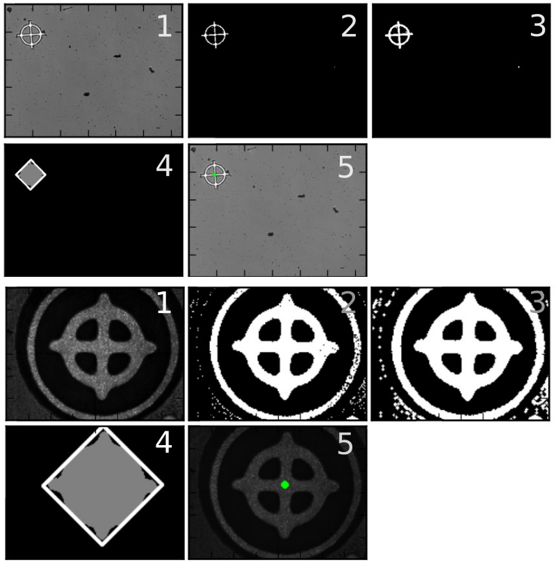
An important feature of the software to aide automation is to automatically extract fiducial locations from images taken by the gantry head camera. An algorithm[@gvision] was designed and implemented with the OpenCV[@opencv_library] computer vision library. [@Fig:fid_recognition] shows the important steps in the algorithm for some representative fiducials. Because this algorithm is implemented in C++, it and its LabVIEW wrappers are bundled separately from the rest of the gantry software[@gvision].
- Acquire an image from the gantry head camera. The algorithm works best if the fiducial is completely withing the camera's field-of-view. Because of this, it is important to have parts placed consistently on the gantry table at least to the 100$\mu \mathrm{m}$ level to be reliably within the roughly 1 mm by 1 mm field-of-view of the camera.
- Apply the K-means clustering algorithm to group pixels based on their brightness. For the BBM fiducials, the fiducial appears bright white on a generally gray background with black flecks. This implies that the K-means clustering should attempt to find three groups where the brightest group of pixels is the fiducial while the other two are background. For the HDI fiducials, there are really only two color groups: black and gray. Therefore, in this case K-means is instructed to only attempt to make two groups. Again, the brighter of the two groups is the fiducial and the other group is background. In both cases, the end result is a binary image with only black and white pixels.
- It is important to have closed shapes. To help with this a "dilate" operation is performed. This operation takes each white pixel and make its neighbors within a certain radius white as well. This acts to close small holes in the foreground resulting from the texture of the fiducial.
- After step 3, there are potentially several blobs of white on a black background, only one of which is the fiducial. To pick out the fiducial, the area and aspect ratio of each blob is calculated and if either lies outside of a prescribed range it is discarded. These ranges are tuned to consistently select only the fiducial and no other random blobs in the image. To provide tolerance to rotated fiducials, the aspect ratio is calculated from a minimum-bounding-box (the white rectangle).
- Finally, the centroid of the remaining blob is calculated and returned as the position of the fiducial in the image.
 {#fig:fid_recognition}
Another necessary function of the software is to calculate from the fiducial position the center and orientation of the parts in the gantry coordinate system. The problem can be phrased like so: given a set of coordinates of reference points in a local Cartesian coordinate system and a corresponding set of measurements of these reference points in the global Cartesian coordinate system, find a coordinate system transformation, $\mathbf{x}' = \mathbf{A} + R\mathbf{x}$, such that the distance between the local coordinate system points and the transformed global points is minimized. In two dimensions, a simple linear regression can be done to find the offet, $\mathbf{A}$, and the rotation matrix, $R$, but in three dimensions such an approach suffers from numerical instability near the poles of the spherical coordinate system. Therefore a more sophisticated algorithm is needed. There are many algorithms that solve this problem[@Tegopoulou2011], but Horn's method[@horn1987] was chosen due to its simplicity and available reference implementations.
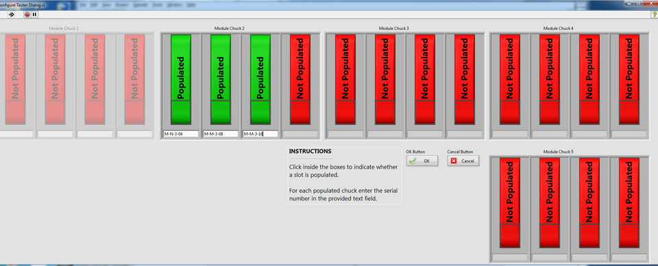
Because the encapsulation routine of the original software was causing issues in production, it was the first candidate for a rewrite using the library of functionality outlined here. Further implementation details of this new application are outside the scope of this document, but [@fig:gui_configure_tester;@fig:gui_review_fiducials;@fig:gui_review_HDI_pads;@fig:gui_align_needle;@fig:gui_summary] follow a walkthrough of an encapsulation session as it would appear to the operator.
 {#fig:gui_configure_tester}
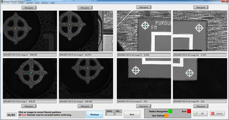 {#fig:gui_review_fiducials}
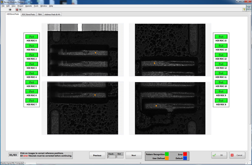 {#fig:gui_review_HDI_pads}
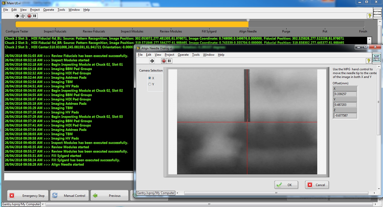 {#fig:gui_align_needle}
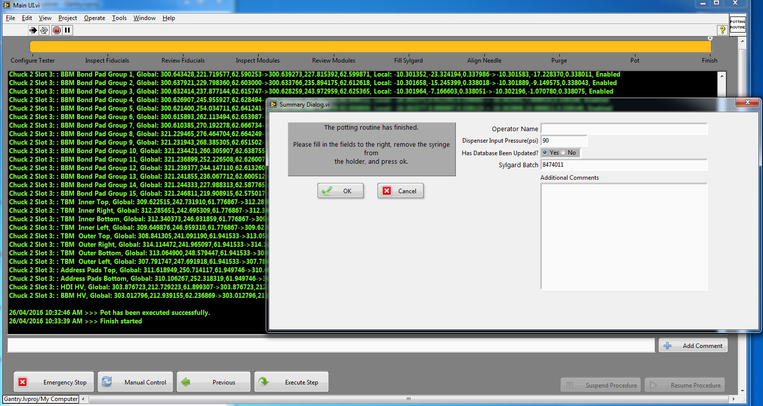 {#fig:gui_summary}
After roughly two months of development, the new encapsulation routine was deployed in production and immediately improved throughput and reliability of encapsulation. It went on to successfully encapsulate modules for the rest of production and served as a useful pattern upon which to develop a new gluing routine.
This same framework is currently being iterated upon for deployment at several assembly sites for the Phase II upgrade of CMS.
Quality Control
An important feature of the encapsulation application is that it keeps a log file containing information such as the serial numbers of modules that were encapsulated, their measured positions, the sections to be encapsulated, and so on. A utility was written to extract information from these log files to measure the quality of alignment during the gluing routine. [@Fig:qc_rotation] shows one of these quality metrics. This is for modules that were assembled by the initial gluing routine, before the rewrite of the gluing routine was finished. It shows a pattern consistent with an incorrect rotation correction, meaning that when the HDI is rotated to match the rotation of the BBM during gluing, that rotation is incorrect. Indeed, upon further investigation it was found that there was a sign error in the rotation correction, leading to the rotation actually being worsened by the "correction". This went unnoticed previously because the correction is normally so small, it is imperceptible to a casual observer.
 {#fig:qc_rotation}
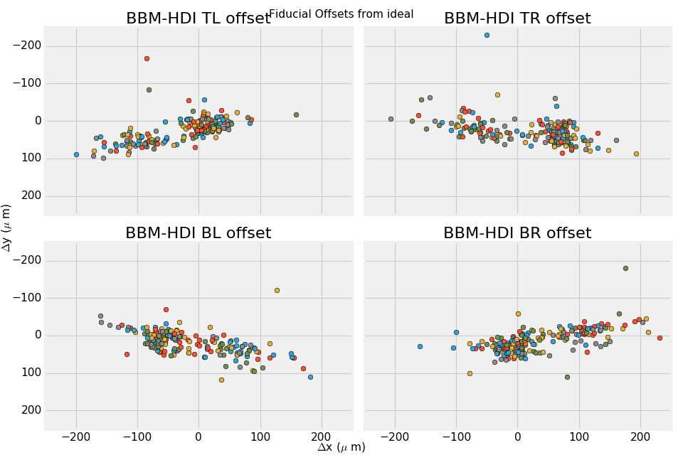
Another example of information that could be gleaned from the encapsulation log files is discovering changes in raw materials. For example, by plotting the post-fit positions of fiducial markings on HDI and separating them by vendor, we found that the HDI produced by Compunetix were out-of-spec by roughly 70 $\mu \mathrm{m}$ as shown in [@fig:qc_vendor].
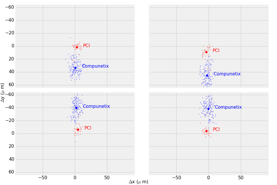 {#fig:qc_vendor}
The assembly precision that was ultimately achieved using the gantry and associated tooling and software are shown in [@fig:gluing_precision;@fig:gluing_precision_rot].
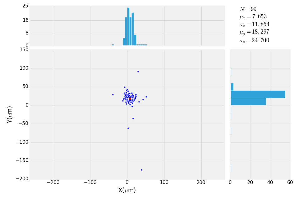 {#fig:gluing_precision}
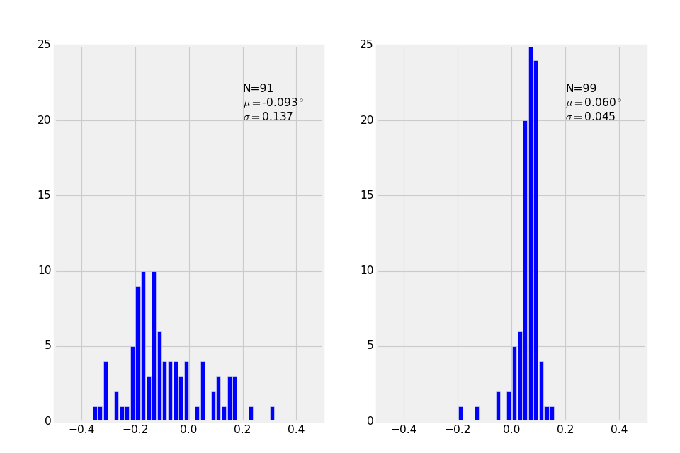 {#fig:gluing_precision_rot}
The Phase II telescope
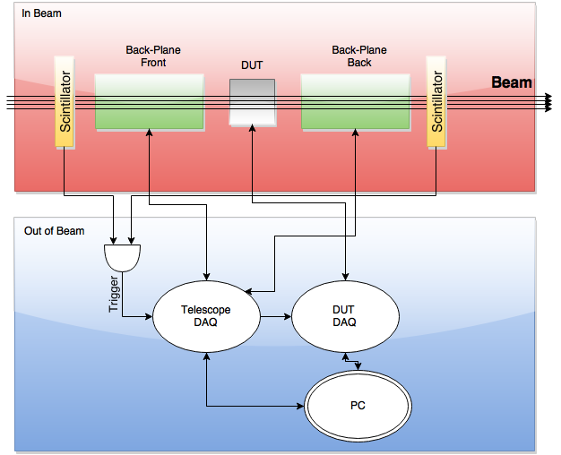
In anticipation of test beams to commission detector elements of the Phase II Upgrade of the CMS detector, a telescope was designed by this author to precisely measure the trajectories of particles in the test beam to serve as a reference when evaluating the performance of a device under test (DUT). The design of the telescope is centered around several layers of silicon strip sensors placed fore and aft of the DUT. Hits in the strips are correlated to construct a track. This track is then projected onto the DUT, and the distance between the impact position of the projected track and the position reading from the DUT form a residual that can characterize the DUT.
[@Fig:telescope_hierarchy] shows a block diagram of the operation of the telescope.
 {#fig:telescope_hierarchy}
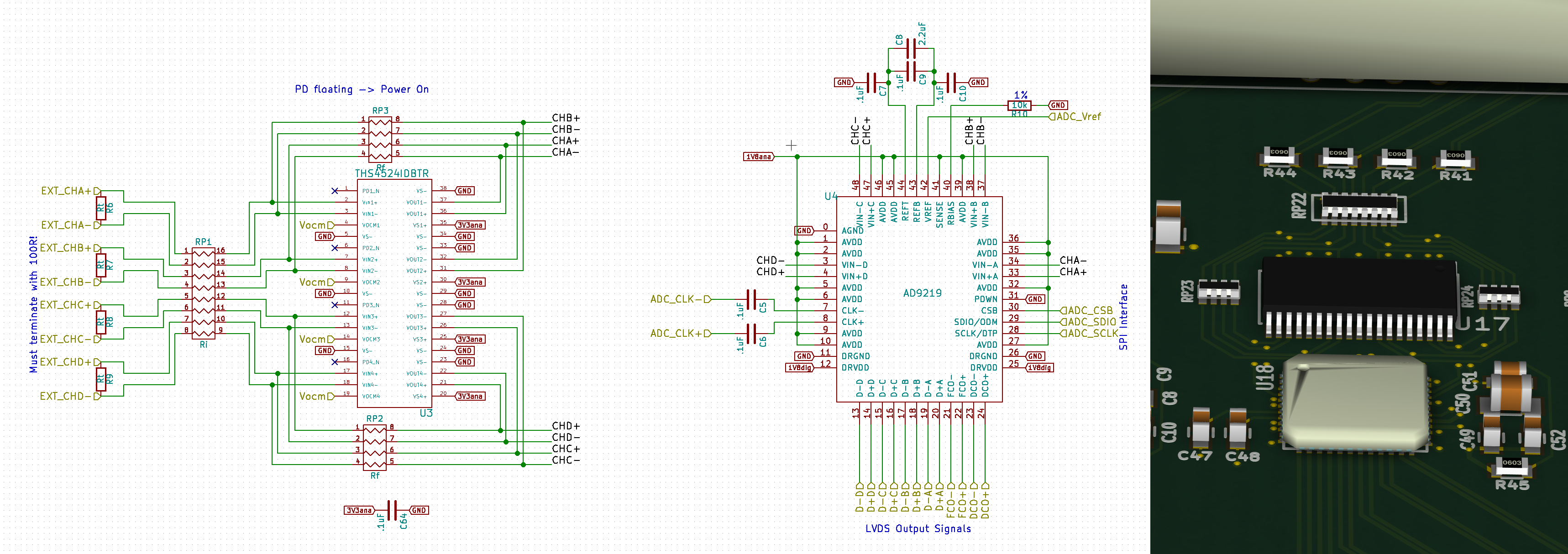
Detector and Readout Chip
The telescope's several layers of sensing material consist of silicon micro-strip sensors. These particular sensors are composed of 512 strips with 25 $\mu$m pitch. The metalization that defines the strips has readout pads on alternating sides of the chip leading to 50 $\mu$m pitch on the pads along either side. [@Fig:telescope_sensor] illustrates this pattern.
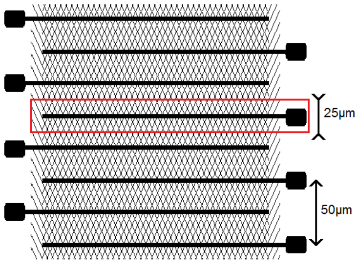 {#fig:telescope_sensor}
The sensor is read out with an integrated circuit called the Analog Pipeline Chip - 128 (APC128). Each APC128 is has a 128 channels which correspond to reading out 128 strips of a silicon micro-strip sensor. [@Fig:apc128] shows an operational schematic detailing one of these channels. Going from left to right, the circuit consists of a pre-amplifier, the sampling capacitors, and readout pipeline.
 {#fig:apc128}
When the APC128 is in sampling mode $SR$ is high, meaning that the switches labeled $SR$ are closed and the switches labeled $\bar{SR}$ are open, and $IS$ is high. We also assume that $Reset$, $R12$, and $CS$ are low. In this configuration any current originating from In flows onto $C_1$. The pre-amplifier will sink the charge that was removed from the right "plate" of $C_1$ to keep it electrically neutral. In the end, the pre-amplifier now has a voltage to maintain on its output that is proportional to the charge read from the sensor. If the $R12$ signal is pulled high by external control circuitry, some of the charge from $C_1$ is allowed to bleed off over time so the voltage of the pre-amplifier will spike with input current and slowly return to its original value. $R12$ also keeps leakage current from saturating the pre-amplifier. On the other hand, if $Reset$ goes high, all of the charge is quickly removed and the pre-amplifier immediately returns to its original state. In a testing environment with bunched particles, the $Reset$ signal may be timed with the beam crossing to clear out the channel between bunches. However, if there is ambiguity when particles could potentially arrive, it is useful to keep a series of periodic samples of the input signal and then read out the correct one when a trigger is received.
Each channel has 32 sampling capacitors, labeled $C_p$ in the schematic. A bit is shifted through the "Pipeline shift register" which connects the output of the pre-amplifier to one $C_p$ at a time. When the pre-amplifier is connected to a particular $C_p$, that capacitor gets charged to a voltage proportional to the input signal at that time. As the bit moves through the shift register, it takes a series of 32 samples of the input signal. Having a time series of samples is important because there is generally a time delay between when the signal from the sensor arrives and when a trigger makes its way through the trigger system to the chip. Without a history of samples, the pulse height information will be lost by the time a trigger arrives.
When a trigger arrives, sampling of the input stops. A specific $C_p$ is selected with the pipeline shift register based on a pre-calibrated trigger delay, and the $SR$ and $IS$ signals go low. This hooks up the $C_p$ capacitor back to the input of the pre-amplifier. A bit is shifted into the "Readout shift register" which connects each of the 128 channels sequentially to the output stage. When a particular channel is connected to the output stage, the pre-amplifier charges the $CL$ capacitor which in turn places a voltage across $C{fb}$ and causes the output amplifier to supply an analog voltage that is proportional to the magnitude of the original pulse from the silicon micro-strip sensor. As the bit in the readout shift register works its way through the channels, a series of analog voltages are supplied to the output which ultimately represent the charge deposits on each of the 128 strips the particular chip is connected to.
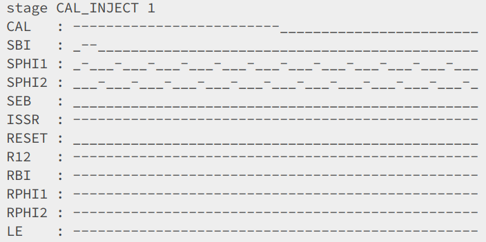
For calibration and testing, the input of the pre-amplifier is given a charge through the $CAL$ input. There is a separate $CAL$ capacitor for each channel with values that cycle starting with C, then 2C, 3C, 4C, and back to C. The different capacitor values give different charge inputs to the pre-amplifiers for a shared calibration voltage. As the different channels are read out, the analog output voltage will step through four discrete values corresponding to the four different capacitor values. [@Fig:step_curve] shows a typical example of this "step curve".
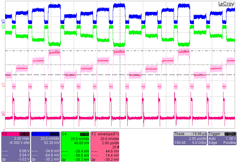 {#fig:step_curve}
The APC128 was originally developed for the HERA experiment at DESY[@Hilgers2001] in the 1990s. In the decades since, much expertise on the operation and performance of the chip has been lost, and very little technical documentation is available. Therefore, in order to better understand the operation of the chip, this author designed a dedicated testboard as part of the telescope R&D. [@Fig:step_curve] was acquired with the aide of this test board, an image of which is shown in [@fig:apc128_testboard].
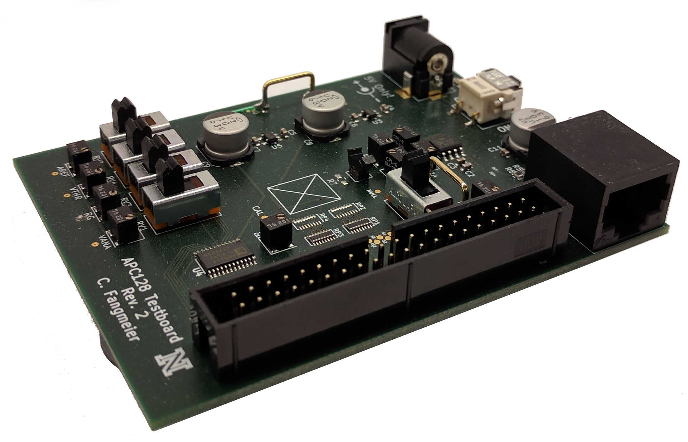 {#fig:apc128_testboard}
Developing the signal patterns that correctly operate the chip to produce the step curve was a significant achievement. This is because even a small error in the pattern can result in erroneous output, with little indication of exactly which signal was wrong and at which clock cycle. To aide in the development of the control signal patterns, software was developed by this author to convert a simple text-based representation of the pattern to FPGA firmware that would actually generate those patterns. [@Fig:apc_pattern] shows an excerpt from one of these patterns. A "-" indicates that the digital signal is high during a clock cycle while a "_" indicates it is low. This excerpt shows the pipeline selection bit being shifted through the pipeline shift register of the APC128 while at some point the CAL signal goes from high to low, injecting some charge into the pre-amplifier. The pre-amplifier will then charge up the currently selected pipeline capacitor. A following section of the pattern will select this capacitor for readout and shift through all 128 channels, producing the step curve.
 {#fig:apc_pattern}
Studies were also done to observe the shape of the pulse when charge is injected into the pre-amplifier via the calibration capacitor. This is shown in [@fig:pulse_decay]. The plot clearly shows the increasing magnitude of the output signal with increasing calibration capacitance, as well as the decay of the signal when the feedback resistor is enabled.
 {#fig:pulse_decay}
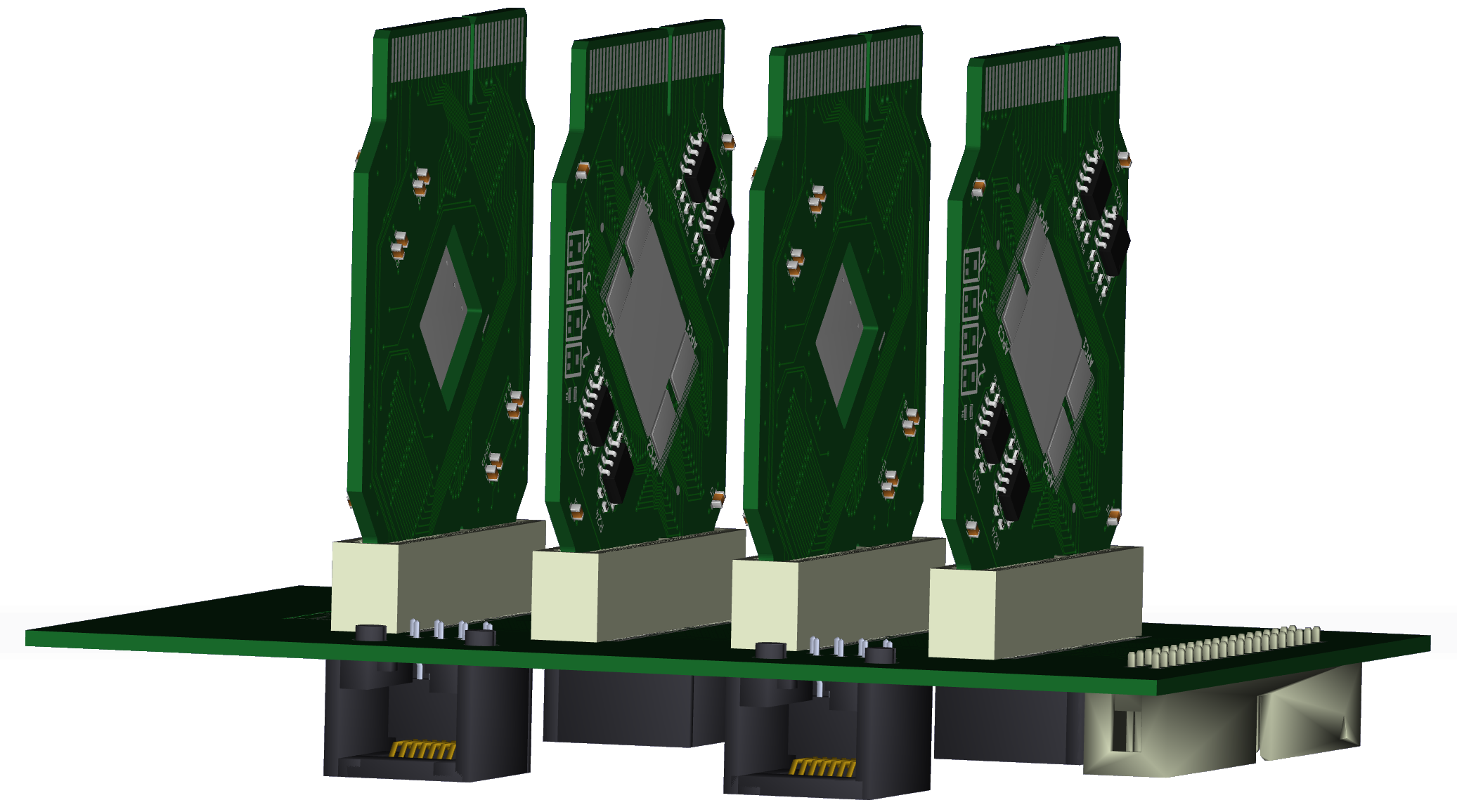
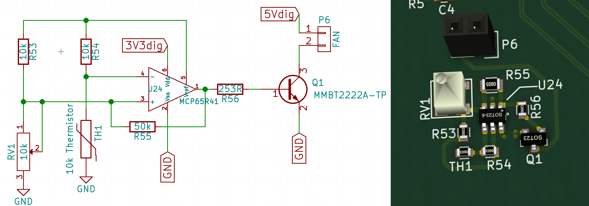
The design of the telescope calls for four layers of detector on each side of the DUT. Each layer will contain one silicon micro-strip detector with four APC128 chips to read out all 512 strips. The analog output of the APC128 has relatively high impedance[@Ryser2013] which implies the need for a nearby amplifier to drive the signal through the connections that lead out of the beam area to the data acquisition board (DAQ). This may be a distance of up to several meters, depending upon the beam site. Based on these requirements, the AD8138ARZ differential amplifier was chosen to drive the signal and twisted pairs in a CAT-5 (i.e. Ethernet) cable were chosen to carry the signal. The board that carries the micro-strip detector, APC128, and amplifiers is referred to as a sensor card. There are four sensor cards mounted onto each of two identical back-plane boards as shown in [@fig:back_plane_board].
The back-plane board would be physically mounted to supports to hold the sensors in the beam path. It has four RJ-45 ports for the CAT-5 cables that route the differential analog signals to the DAQ and a 2x20 parallel connector for the DAQ to supply the APC128 control signals, bias voltage, and other miscellaneous signals required by the sensor cards.
 {#fig:back_plane_board}
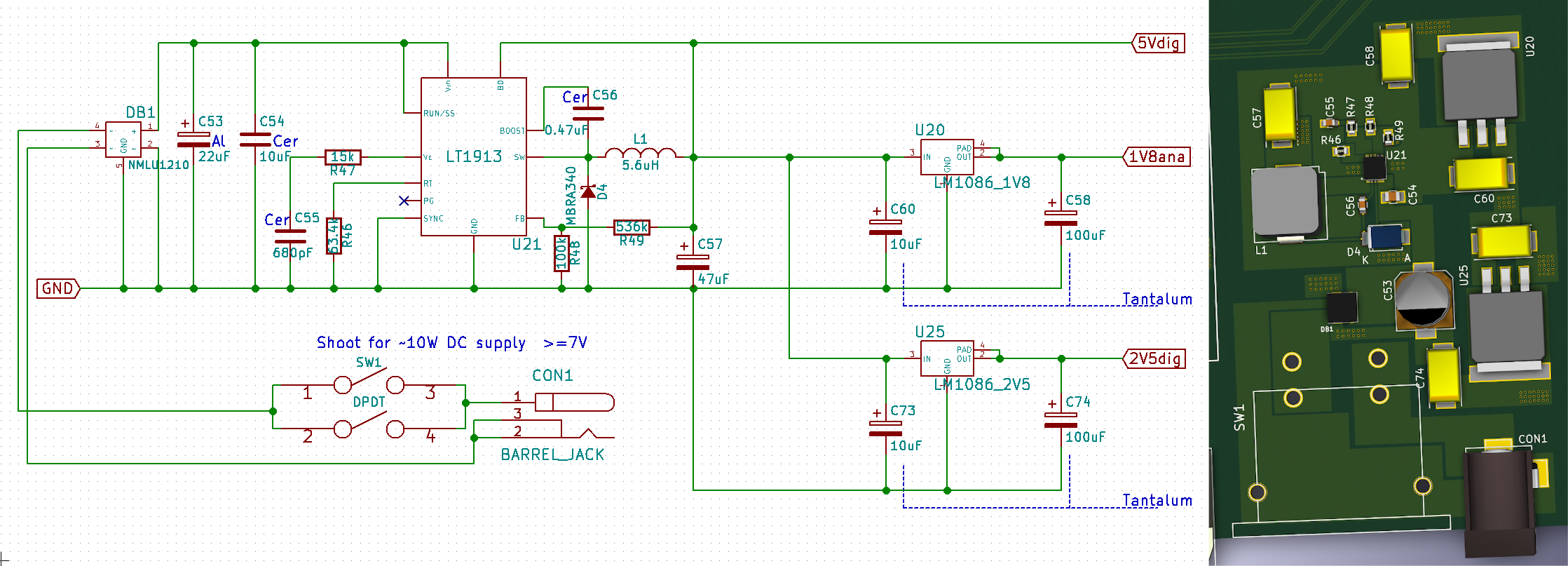
Data Acquisition Board
The DAQ has four main functions:
- Generate the control patterns for the APC128. This includes the pattern to continuously sample the pre-amplifier and the pattern to select the correct sample from each channel and readout the samples.
- Digitize the analog signals coming from the 32 APC128 chips. To minimize downtime during readout, all 32 are digitized in parallel.
- Pre-process the readings to suppress noise and identify hits.
- Transmit the collected hit data to a connected PC for further processing and storage.
To accomplish these goals, a DAQ board, shown in [@fig:daq_overview], was designed and built. Not shown in the figure is the brains of the board: an Opal Kelly ZEM4310 FPGA integration board. The ZEM4310 plugs into the two central HSMC connectors which connect the FPGA to power, the ADCs, the APC128 control pattern lines, and other utility circuits. The ZEM4310 was chosen for its high amount of I/O, USB3 connectivity, and, importantly, its use of an Altera FPGA, a part that the DAQ designer already had experience programming.
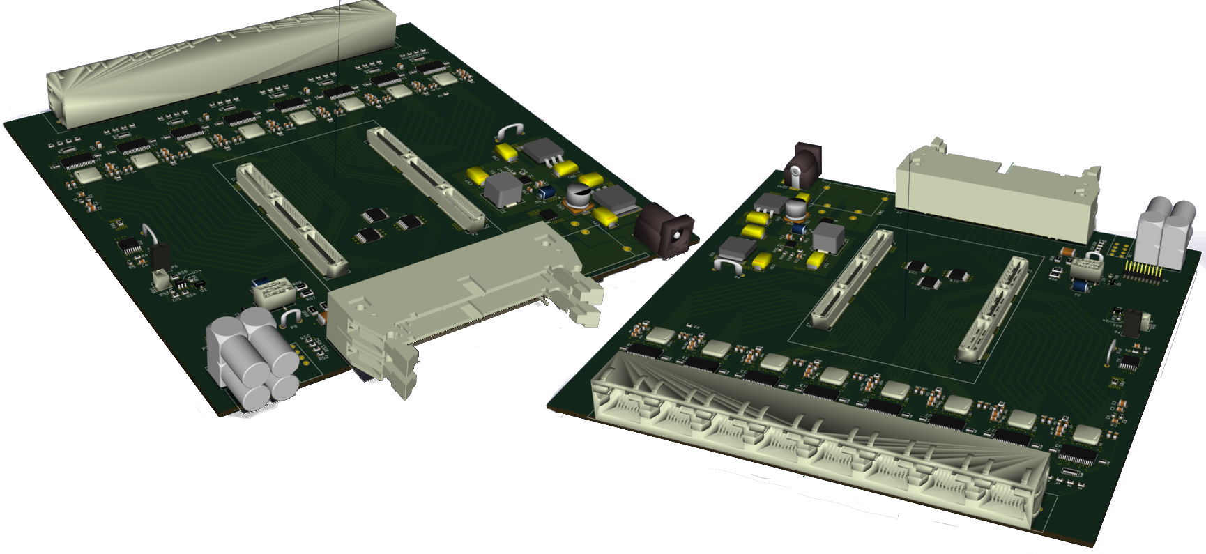 {#fig:daq_overview}
 {#fig:daq_fan_control}
 {#fig:daq_single_channel}
 {#fig:daq_power}
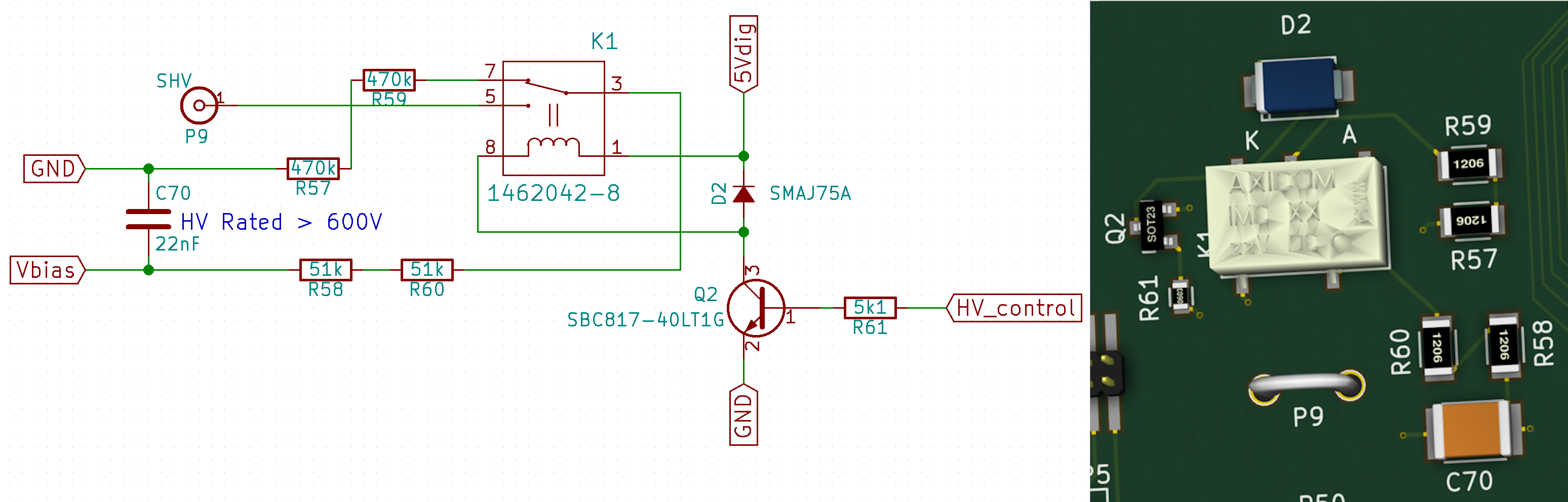 {#fig:daq_hv_control}
Software
An FPGA is a dynamic and programmable piece of hardware. Unlike devices like micro-controllers, however, an FPGA is able to directly emulate bare-metal logic circuits. This means that specialized digital circuits can be designed to handle specific tasks quickly, efficiently, and in parallel. The downside of this, however, is that FPGAs cannot be programmed with a typical programming language like C or Python, but instead use a special hardware design language. There are two popular language choices for FPGA design: Verilog, and VHDL. There is also a "block diagram" visual style of programming that some IDEs support. For the DAQ software, Verilog was chosen due to its more "C-like" syntax over the more verbose VHDL. [@Fig:verilog_sample] shows a sample of some Verilog code.
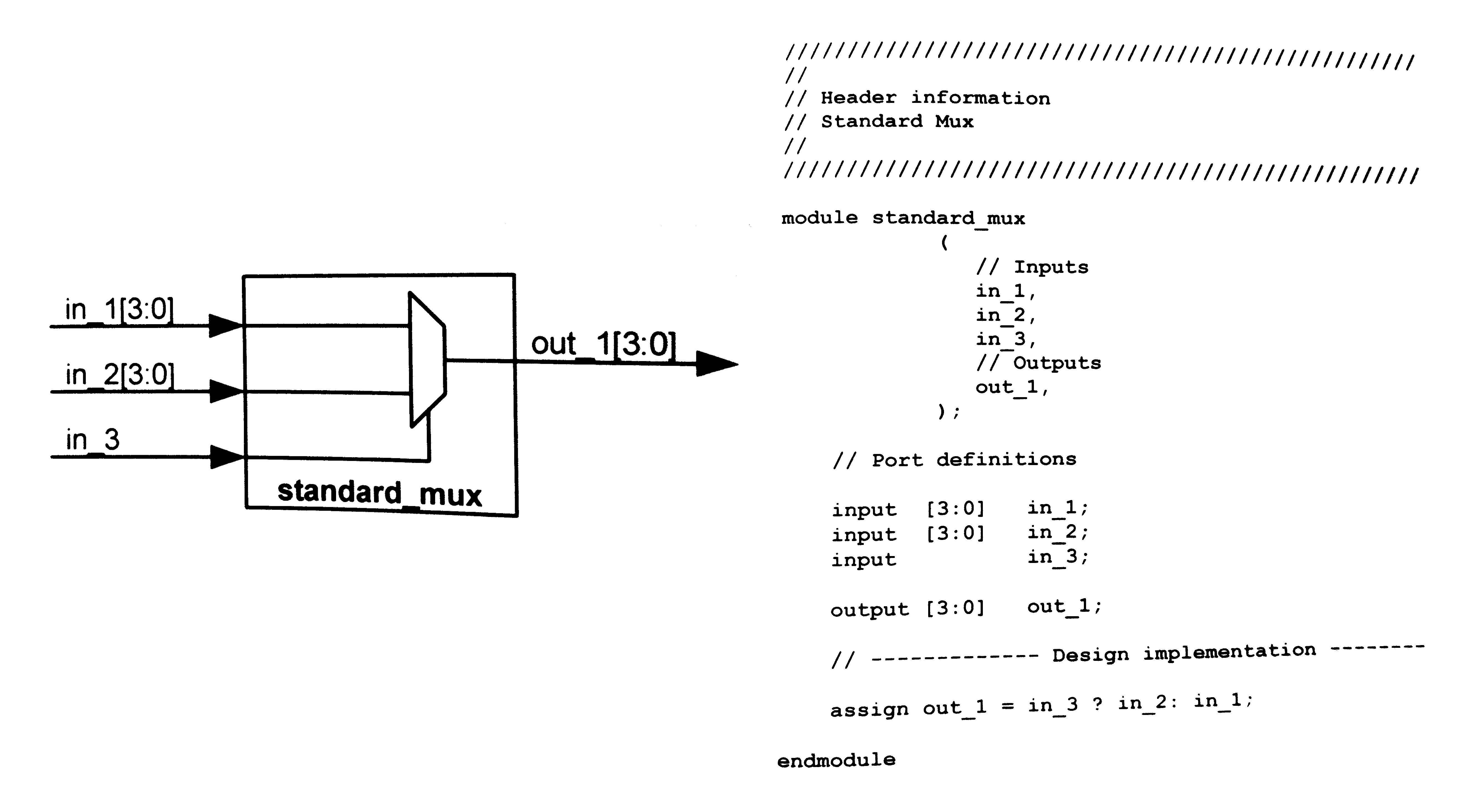 {#fig:verilog_sample}
Although one could, in principle, construct all of the necessary functionality of the DAQ firmware with Verilog logic circuits, it would be rather inflexible, requiring time-consuming recompilation and synthesis of the design upon any minor change. This motivates the need for "software" that can be loaded into the ZEM4310's RAM and then executed by logic on the FPGA. This is exactly what was done. A simple RISC (reduced instruction set computer) processor was implemented in Verilog. This processor implements a custom instruction set and uses memory mapped I/O to allow for access to the RAM, the ADCs, the lights on the RJ-45 connector, and so on. In this way, software could be developed that would orchestrate the operation of the DAQ. The software could also be changed on the fly during operation and testing by simply updating the content of a portion of the RAM and resetting the processor. An assembler was also written to convert human readable assembler code to the binary machine code used by the processor[@daq_software].
To facilitate communication between the FPGA and a connected computer, Opal Kelly provides a set of firmware blocks that can be incorporated into the FPGA design that interface with the USB3 controller to send and receive data from the host PC. Similarly, they have written PC software that couples to these signals and provides a simple programming interface in many popular programming languages, including Python.
Outlook
As of the time of this writing, the sensor layer cards, backplane board, and DAQ hardware[@daq_hardware] are finished. The DAQ firmware and software are developed as described in this document, however additional work is necessary to enable use in a test beam.